
Motivation
Various algorithms such as matrix multiplication and attention that AI workloads employ are highly parallelizable by design, and thus use specialized silicon such as Graphics Processing Units (GPUs) or Tensor Processing Units (TPUs). GPUs began as fixed-function hardware designed solely to accelerate the rendering of pixels and 3D geometry for video games. They evolved into fully programmable parallel processors, enabling developers to harness their massive throughput for general scientific computing and AI workloads.
NVIDIA has emerged as the largest supplier of GPUs, cemented by the development of the CUDA ecosystem, which is highly optimized, easily integrates with popular libraries and frameworks, and allows ease of development.
In this blog, we are going to discuss the architecture of NVIDIA GPUs and CUDA. This is not an introduction to CUDA programming, though we make reference to simple CUDA programs to explain the CUDA execution and hardware architecture. We will explore how things work under the hood, which might or might not be useful for writing CUDA kernels, but is interesting to know nonetheless.
GPU: The Throughput Machine
FLOPS and Bandwidth
You might have heard a supercomputer’s power being stated in terms of FLOPS (FLoating point Operations Per Second). For instance IIT Kanpur’s HPC 2013 has a Rmax rating of 344.3 TeraFLOPS. However it turns out that memory bandwidth is what we should care about more.
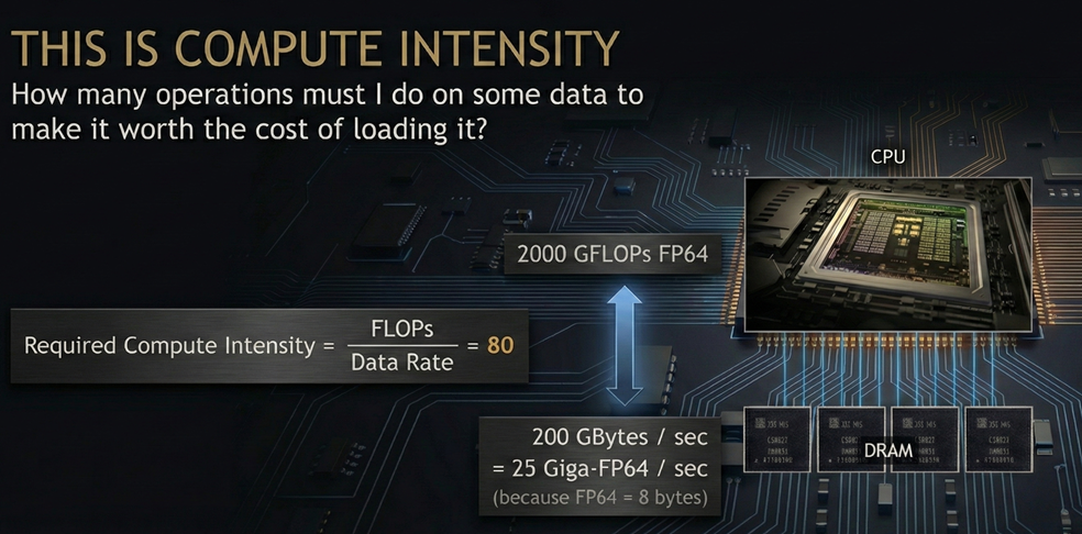
The compute intensity of 80 in the above example means that at least 80 operations must be done on each bit of data loaded. Otherwise I am not keeping my processor busy, and a cheaper CPU should have sufficed. In fact there are not many algorithms which have so much to do on every piece of data, in fact there is only one extremely important one: matrix multiplication.
Latency: The main bottleneck
Memory latency turns out to be the main bottleneck to utilizing all the FLOPS in the machine. Memory latency is the physical time delay between a processor requesting a piece of data and that data being delivered and ready for use. Latency is caused by data being transferred from one bank of transistors to another as it steps through all the logical operations, and turns on and off at the clock rate. To understand why, let’s look at a standard DAXPY (Double-precision AX+Y) operation running on an Intel Xeon 8280.
Case Study on DAXPY
DAXPY is a very common instruction and processors have an instruction FMA (Fused Multiply Add) that does it in a single instruction.
//Pseudocode for DAXPY
void daxpy(int n, double alpha, double *x, double *y)
{
    for (i = 0; i < n; i++)
    {
        y[i] = alpha * x[i] + y[i];
    }
}
The Intel Xeon 8280 has a memory bandwidth of 131 GB/s and a loaded latency of approximately 89 nanoseconds. In the time it takes for a single memory request to return, the system’s bandwidth is theoretically capable of moving 11,659 bytes of data. A single iteration of DAXPY only loads two double values, totaling 16 bytes. In this state, the memory efficiency is only 0.14%. In order to keep the memory bus busy, multiple (here 729) iterations of DAXPY must be run at once.

Compilers and hardware employ pipelining. The goal is to issue memory loads as early as possible so that the “wait time” is overlapped with useful work, such as the multiplication of a and X. Pipelining is the core of most program optimization.
Concurrency helps maintain multiple operations “in flight” simultaneously. Techniques like loop unrolling allow a single thread to issue multiple independent memory requests back-to-back, attempting to fill that latency gap with more data.
//Loop unrolling pseudocode
void daxpy(int n, double alpha, double *x, double *y)
{
    for (i = 0; i < n; i += 8)
    {
        y[i+0] = alpha * x[i+0] + y[i+0];
        y[i+1] = alpha * x[i+1] + y[i+1];
        y[i+2] = alpha * x[i+2] + y[i+2];
        y[i+3] = alpha * x[i+3] + y[i+3];
        y[i+4] = alpha * x[i+4] + y[i+4];
        y[i+5] = alpha * x[i+5] + y[i+5];
        y[i+6] = alpha * x[i+6] + y[i+6];
        y[i+7] = alpha * x[i+7] + y[i+7];
    }
}
Concurrency is limited by the amount of “outstanding” work a single thread can track—once it hits its buffer limit, it must stop and wait. On the other hand, parallelism distributes operations across thousands of threads.
//Pseudocode for parallelism
void daxpy(int n, double alpha, double *x, double *y)
{
    parallel for (i = 0; i < n; i++)
    {
        y[i] = alpha * x[i] + y[i];
    }
}
Throughput vs Latency
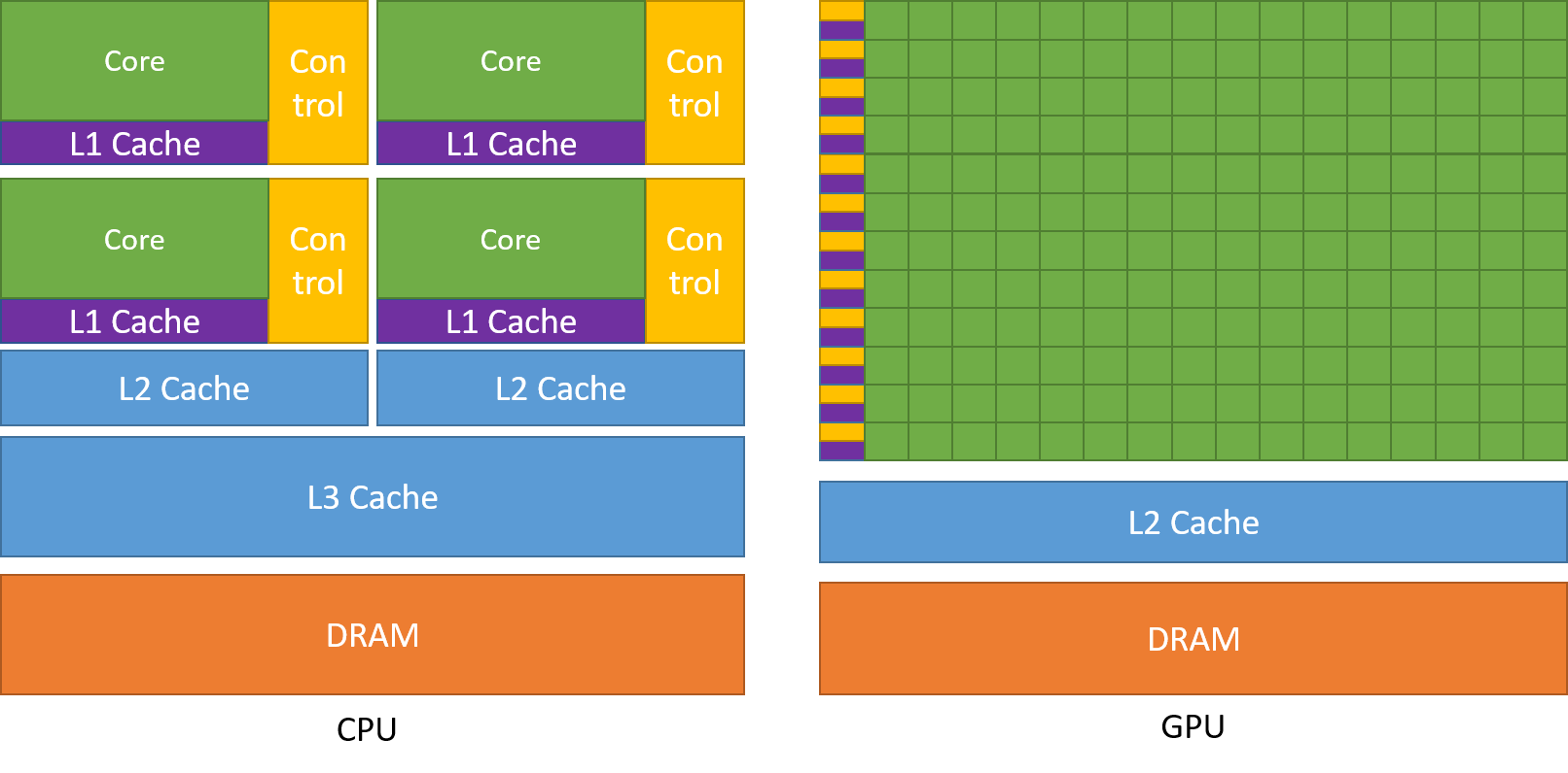
CPUs are designed as latency machines, allocating a significant portion of their hardware to massive caches to minimise the memory latency. The expectation of the CPU is that a single thread is largely doing all of the work. It is expensive to switch out these threads for another, as it necessitates saving and restoring execution states to off-chip memory. A CPU needs just enough threads to cover the latency. Conversely, GPUs function as throughput machines that hide high latency through oversubscription, keeping thousands of threads alive so that when one execution group stalls, the system always has other work ready to proceed. This strategy is enabled by zero-overhead context switching, allowing the hardware to swap execution between threads in a single clock cycle without moving data. This efficiency is possible because the GPU features a massive, persistent register file that keeps every thread’s state resident on the chip throughout its entire lifecycle.
To mitigate any confusion, we draw a simple analogy between a car and a train. A car is a latency machine, it’s optimised to take me from point A to point B, but it doesn’t really help anybody else. A train on the other hand, can carry lot of people, it stops at a lot of places, and we can have multiple trains along the route. A train is therefore a throughput machine. Latency systems perform horribly if they are oversubscribed: if there are too many cars there is a traffic jam. In contrast, a GPU is underutilized if it is not oversubscribed just as a train company loses money if the trains are not full.
GPU Architecture
Core hardware components
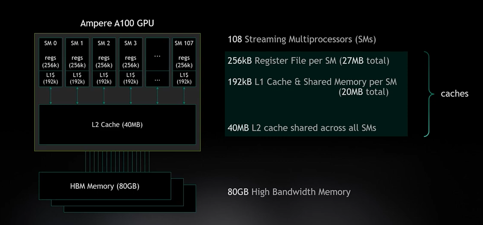
Modern NVIDIA GPUs are built around a set of scalable Streaming Multiprocessors (SMs), which serve as the primary processing units. Each SM contains hundreds or thousands of smaller cores, including units for integer arithmetic, floating-point operations (FP32, FP64), and Tensor Cores specifically designed to accelerate matrix multiplications for AI. GPUs possess a massive, persistent register file that is significantly larger than those in CPUs (often megabytes rather than kilobytes). This allows the hardware to keep the state of thousands of threads active on the chip simultaneously. To handle the immense data requirements of its cores, GPUs utilise High Bandwidth Memory (HBM) and a hierarchical cache system (L1/L2), though a significant gap remains between what the cores can request (up to 10 TB/s) and what the memory system can provide (approx. 1.5 TB/s)
SIMT execution
GPUs employ a unique architecture called Single Instruction, Multiple Threads (SIMT). Unlike SIMD (Single Instruction, Multiple Data), which operates on fixed vectors, SIMT allows each thread to have its own independent state, registers, and program counter. Threads can loop or branch independently; however, if threads within the same execution group follow different paths, the hardware must serialize those branches, a phenomenon known as branch divergence that can reduce efficiency. In the CUDA programming model, work is organised into a hierarchy of threads, blocks, and grids. While these are abstractions for the programmer, the hardware executes them in groups of 32 consecutive threads known as warps.
DRAM / VRAM
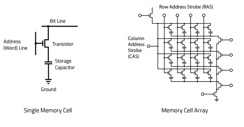
A cell on the left can store a bit (on or off) indicated by the charge on the capacitor. In a DRAM chip, we have millions of these cells connected in a big 2D grid. This matrix layout allows access to any row/column, allowing random access of data. Data is accessed as follows:
- The row address is activated and the state of all the cells are copied to a sense amplifier. This destroys the data in the rows as the capacitors are drained.
- Required data is read from the row held in the amplifiers. This does not destroy the data in the amplifiers.
- Thus we can make multiple reads at different column indices from the data held in the amplifiers.
- Before a new row is fetched, the old row must be written back because the old row was destroyed.
From the above mechanism we’d expect that reading continuous chunks together is faster, and this is indeed the case. To state the obvious, data access patterns really matter! For example, in most programming languages, 2D arrays are stored row-wise. Hence accessing them column-wise would be much slower.
Why warps?
Consecutive threads are grouped into 32 threads, so that contiguous data can be accessed simultaneously. Although an A100 GPU can handle 64 warps in a SM, only 4 can run at a time. Suppose a thread reads 8 bytes of data from a particular segment. Therefore we are accessing a chunk of 1024 (32 $\times$ 4 $\times$ 8) bytes, which turns out to be be the size of an entire row in the HBM (RAM).
CUDA Framework
CUDA (Compute Unified Device Architecture) is a proprietary parallel computing platform and programming model developed by NVIDIA, first launched in 2007. CUDA is both a software layer that manages data, giving direct access to the GPU and CPU as necessary, and a library of APIs that enable parallel computation for various needs. In addition to drivers and runtime kernels, the CUDA platform includes compilers, libraries and developer tools to help programmers accelerate their applications.
CUDA Execution Hierarchy
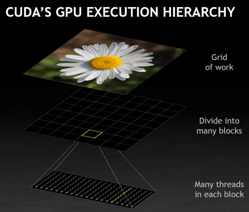
Let us discuss CUDA’s execution policy. Suppose I want to do some image processing on this image of a flower. We divide this data into equal sized blocks comprising a grid of work. Now each of the blocks will run independently and in parallel, and data cannot be exchanged between them. Since there are so many blocks, the GPU is oversubscribed by them. The GPU places each of the blocks in a SM, spreading them out among all available SMs. Placing all the blocks in the same SM, would saturate the memory bandwidth of the SM, hence distributing the blocks across the SMs is a better strategy. The hardware keeps placing blocks onto a SM until it is full. A SM can fit up to 32 blocks. Once a block finishes executing, it exits and another block is placed in the gap. The multiple threads within a block can run independently, but may synchronize to exchange data. As discussed before threads are grouped into a warp consisting of 32 threads.
Anatomy of a CUDA program
A CUDA program is a hybrid. The “Host” (CPU) manages the environment and data, while the “Device” (GPU) performs the heavy lifting.
#define N 10000000

// 1. THE KERNEL
// This function runs on the GPU. Each thread executes this exact code.
__global__ void vector_add(float *out, float *a, float *b, int n) {
    // Calculate global index:
    // "Which block am I in?" * "How wide is a block?" + "Who am I in this block?"
    int i = blockIdx.x * blockDim.x + threadIdx.x;

    // Boundary Check: Ensure we don't write outside the array
    if (i < n) {
        out[i] = a[i] + b[i];
    }
}

int main() {
    // 2. MEMORY ALLOCATION (The Physical Separation)
    float *a, *b, *out;          // Host pointers (CPU RAM)
    float *d_a, *d_b, *d_out;    // Device pointers (GPU VRAM)

    // Allocate 10 million floats in CPU RAM
    a = (float*)malloc(N*sizeof(float));
    b = (float*)malloc(N*sizeof(float));
    out = (float*)malloc(N*sizeof(float));

    // Initialize data on CPU
    for(int i=0; i<N; i++) { a[i]=1.0f; b[i]=2.0f; }

    // Allocate 10 million floats in GPU VRAM
    cudaMalloc(&d_a, N*sizeof(float));
    cudaMalloc(&d_b, N*sizeof(float));
    cudaMalloc(&d_out, N*sizeof(float));

    // 3. THE BOTTLENECK (Data Movement)
    // Move data across the PCIe bus (The "Latency Tax")
    cudaMemcpy(d_a, a, N*sizeof(float), cudaMemcpyHostToDevice);
    cudaMemcpy(d_b, b, N*sizeof(float), cudaMemcpyHostToDevice);

    // 4. OVERSUBSCRIPTION (Launch Configuration)
    // We launch enough blocks to cover all N elements.
    // (N + 255) / 256 is a standard trick to ensure we round UP.
    dim3 blocks((N+255)/256);
    dim3 threads(256);

    // Launch the Kernel: "blocks" trains, with 256 "passengers" each
    vector_add<<<blocks, threads>>>(d_out, d_a, d_b, N);

    // 5. RETRIEVAL
    // Copy the result back to CPU RAM so we can use it
    cudaMemcpy(out, d_out, N*sizeof(float), cudaMemcpyDeviceToHost);

    // Cleanup
    cudaFree(d_a); cudaFree(d_b); cudaFree(d_out);
    free(a); free(b); free(out);
    return 0;
}
- __global__: The keyword that defines a kernel. It tells the compiler “This function runs on the GPU, but is called from the CPU.”
- threadIdx & blockIdx: The built-in coordinate system. Every thread uses these to calculate its unique ID.
- threadIdx.x: “Who am I inside this block?”
- blockDim.x: “How many threads are in a block?”
- blockIdx.x: “Which block is this?”
Running this code
To run this code on your machine having an NVIDIA GPU, you must download the CUDA Toolkit. This is very easy on Ubuntu/Debian:
$~ sudo apt install cuda-toolkit
Refer to this tutorial for setting up CUDA Toolkit on Windows (WSL).
You can now save this program as a .cu file and compile it with the nvcc compiler
The next section discusses how GPUs have revolutionised robotics and fields related to IoT by introducing edge GPU computing
Edge GPUs: Making AI accessible for all devices
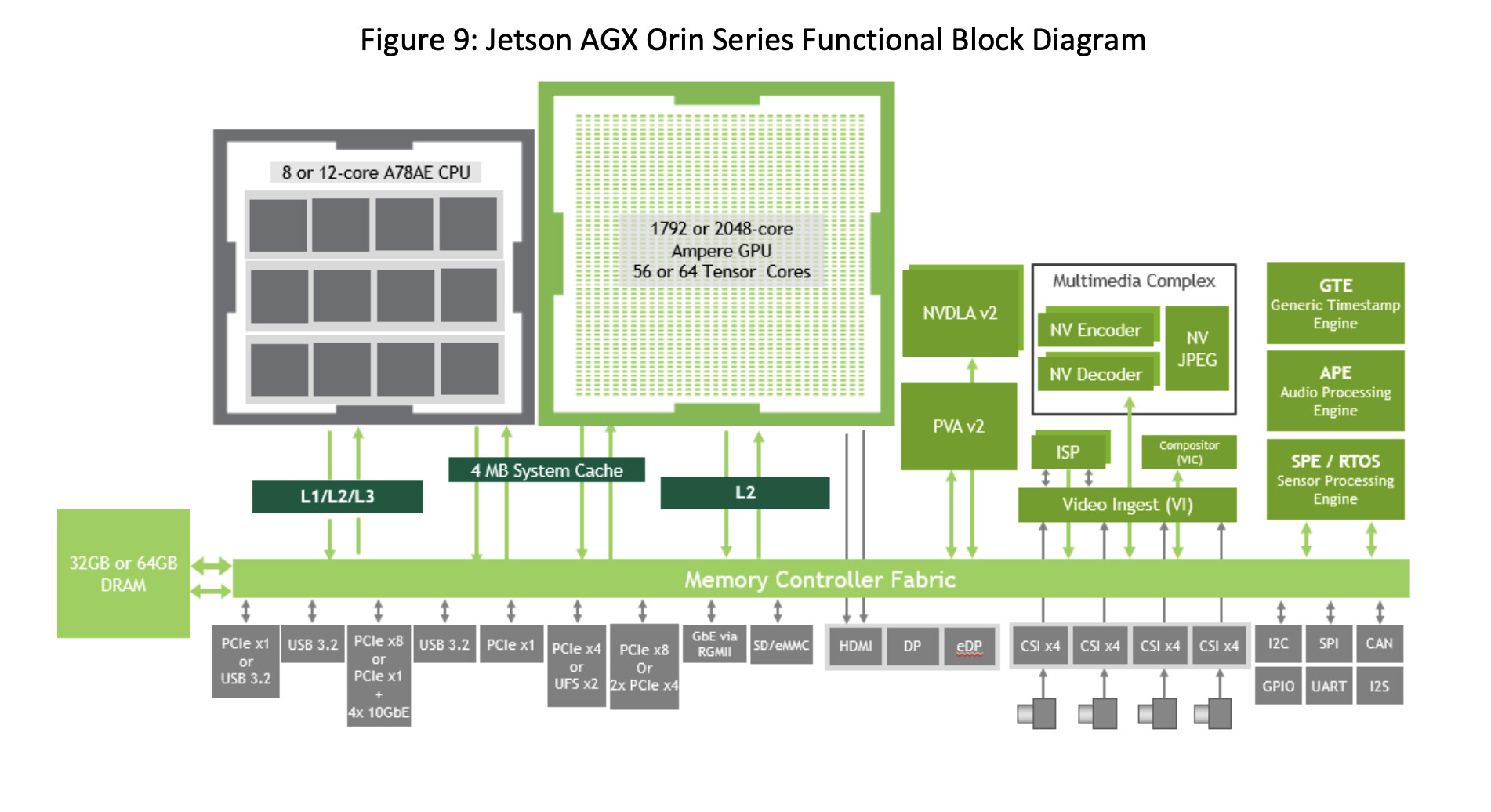
The advancement in chip design and AI has led to development of small yet powerful GPUs which fit in the palm of your hand, these enable very fast compute on IoT devices such as drones or CCTV cameras. This opens up a world of possibilities such as on board image processing via AI models or running millions of parallel processes on devices at the edge of the networm.
What “Edge GPU” Really Means
Most AI workloads today live in the cloud, where latency, connectivity, and privacy are someone else’s problem. Edge GPUs flip that model:
- Local inference: Models run right next to the sensors, so decisions happen in milliseconds instead of waiting on a server.
- Privacy: Raw video, audio, and sensor data stay on‑device, while this not only helps reduce server load, it ensures that the users’ privacy is ensured as well .
- Connectivity‑proof: Works even without constant internet, perfect for drones, autonomous robots, or remote industrial sites.
At a human level, edge GPUs are what has been pioneering the new generation of robots bringing fast reaction times with powerful compute power.
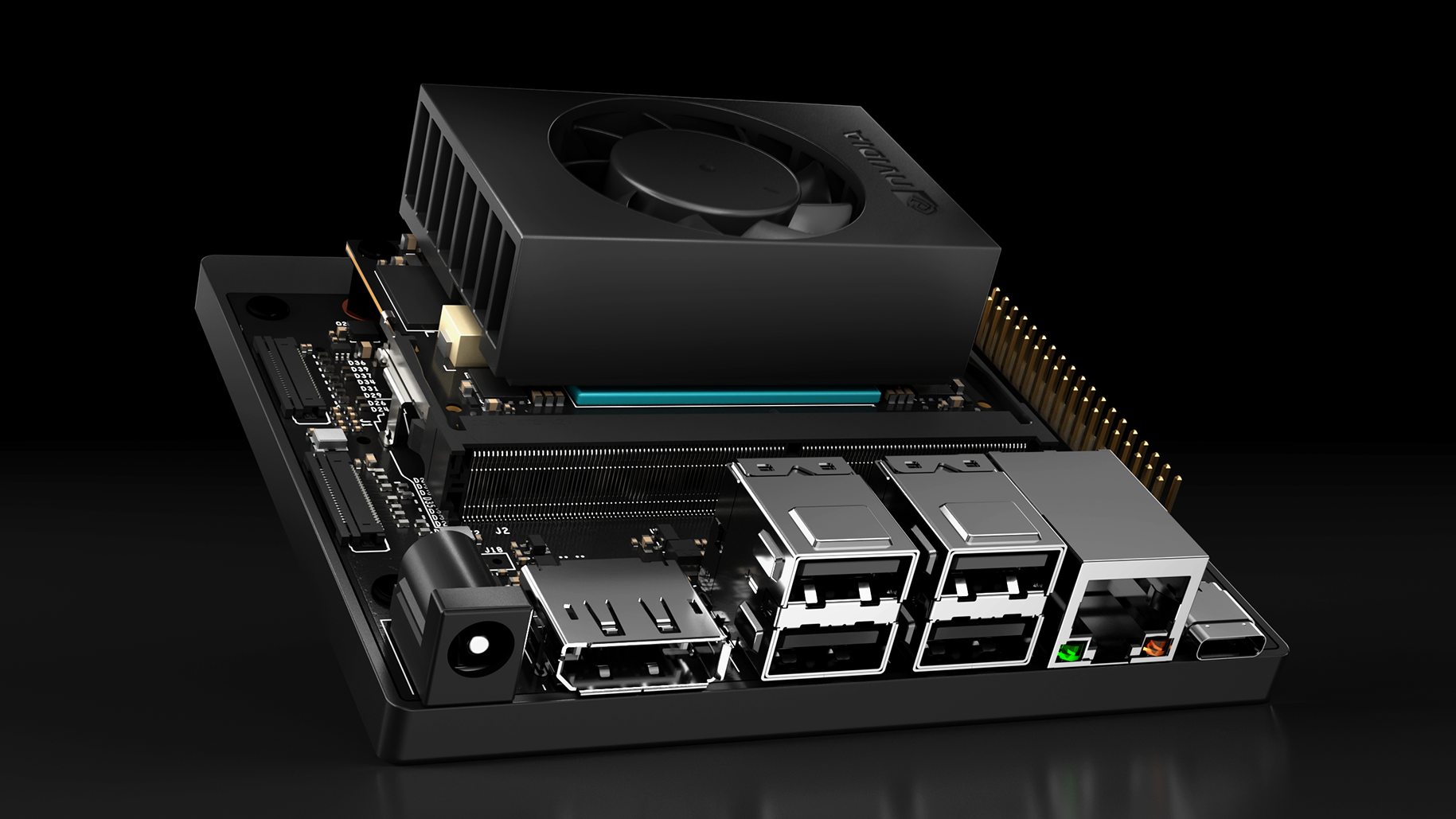
Nvidia Jetson Nano: The current standard for hobbyists and engineers alike to explore edge GPUs
The NVIDIA Jetson Nano is often the first serious step beyond a Raspberry Pi for AI. It’s a compact single‑board computer built specifically for machine learning and computer vision at the edge.
Housing a powerful Quad-core ARM Cortex-A57 CPU with a 128-core Maxwell GPU(about 472 GFLOPS) and a 4GB RAM it is more than capable of:
- Run multiple neural networks in real time (think of object detection, segmentation, or speech processing).
- Power autonomous robots, drones, and smart IoT devices on a simple battery pack.
Current potential of edge GPUs and impact made
Developers and makers have used Jetson‑class boards for some wild edge AI projects:
- Search‑and‑rescue robots: Self‑navigating ground bots that map, detect, and retrieve objects autonomously.
- Fire‑detecting drones: On‑board CNNs spotting early wildfire signatures without streaming raw video to the cloud.
- Smart safety systems: Helmet and mask detection for construction sites, processing camera feeds in real time.
- Assistive tech: Image captioning tools that describe a scene locally
The pattern is always the same: high‑bandwidth sensor data processed locally, with only insights sent upstream.
Why Edge GPUs Matter for the Next Decade
Edge GPUs are reshaping how AI feels in the real world. Instead of “upload and wait,” interactions become immediate, contextual, and resilient.
For builders, that means:
- You can prototype serious AI products on your desk, powered by a laptop charger.
- The same platform scales from a hobby robot to production‑grade autonomous machines.
- You can blend cloud intelligence with edge responsiveness, thereby offloading only what’s necessary.
If you’re into robots, drones, or smart devices, edge GPUs like the Jetson Nano aren’t just another board. They’re the missing piece that lets your ideas leave the simulator and survive the real world.
Authors: Arnab Datta & Pradyumn Vikram